| Symbol | Characteristics | Min. | Typ. | Max. | Units | |
|---|---|---|---|---|---|---|
| VIH | Input High Voltage | 2.0 | Vcc | V | ||
| VIL | Input Low Voltage | -0.3 | 0.8 | V | ||
| IIN | Input Leakage (02, /W/R, /RES, /CS, RS, LPEN, CCLK | - | 2.5 | uA | ||
| ITSI | Three-State Input Leakage (DB0-DB7) VIN = 0.4 to 2.4V |
-10.0 | - | V | ||
| VOH | Output High Voltage | ILOAD = -205 uA (DB0-DB7) ILOAD = -100 uA (all others) |
2.4 | - | V | |
| VOL | Output Low Voltage ILOAD = 1.6mA |
- | 0.4 | V | ||
| PD | Power Dissipation | - | 325 | 650 | mW | |
| CIN | Input Capacitance | |||||
| 02, /W/R, /RES, /CS, RS, LPEN, CCLK | - | 10.0 | pF | |||
| DB0-DB7 | - | 12.5 | pF | |||
| COUT | Output Capacitance | - | 10.0 | pF |
| Symbol | Characteristics | UM6845R | UM6845RA | UM6845RB | Units | |||
|---|---|---|---|---|---|---|---|---|
| Min. | Max. | Min. | Max. | Min. | Max. | |||
| tCYC | Cycle Time | 1.0 | - | 0.5 | - | 0.33 | - | us |
| PWEH | E Pulse Width, High | 440 | - | 200 | - | 150 | - | ns |
| PWEL | E Pulse Width, Low | 420 | - | 190 | - | 140 | - | ns |
| tAS | Address Set-Up Time | 80 | - | 40 | - | 30 | - | ns |
| tAH | Address Hold Time | 0 | - | 0 | - | 0 | - | ns |
| tCS | /W/R, /CS Set-Up Time | 80 | - | 40 | - | 30 | - | ns |
| tCH | /W/R, /CS Hold Time | 0 | - | 0 | - | 0 | - | ns |
| tDSW | Data Bus Set-Up Time | 165 | - | 60 | - | 60 | - | ns |
| tDHW | Data Bus Hold Time | 10 | - | 10 | - | 10 | - | ns |
| Symbol | Characteristics | UM6845R | UM6845RA | UM6845RB | Units | |||
|---|---|---|---|---|---|---|---|---|
| Min. | Max. | Min. | Max. | Min. | Max. | |||
| tCYC | Cycle Time | 1.0 | - | 0.5 | - | 0.33 | - | us |
| PWEH | E Pulse Width, High | 440 | - | 200 | - | 150 | - | ns |
| PWEL | E Pulse Width, Low | 420 | - | 190 | - | 140 | - | ns |
| tAS | Address Set-Up Time | 80 | - | 40 | - | 30 | - | ns |
| tAH | Address Hold Time | 0 | - | 0 | - | 0 | - | ns |
| tCS | /W/R, /CS Set-Up Time | 80 | - | 40 | - | 30 | - | ns |
| tCH | /W/R, /CS Hold Time | - | 290 | - | 150 | - | 100 | ns |
| tDSW | Data Bus Set-Up Time | 20 | 60 | 20 | 60 | 20 | 60 | ns |
| tDHW | Data Bus Hold Time | 40 | - | 40 | - | 40 | - | ns |
| Symbol | Parameter | Min. | Max. | Units | |
|---|---|---|---|---|---|
| TCCH | Maximum Clock Pulse Width, High | 200 | ns | ||
| TCCV | Clock Frequency | 2.5 | Mhz | ||
| Tr,Tf | Rise and Fall Time for Clock Input | 20 | ns | ||
| tMAD | Memory Address Delay Time | 100 | 160 | ns | |
| tRAD | Raster Address Delay Time | 100 | 160 | ns | |
| tDTD | Display Timing Delay Time | 160 | 300 | ns | |
| tHSD | Horizontal Sync Delay Time | 160 | 300 | ns | |
| tVSD | Vertical Sync Delay Time | 160 | 300 | ns | |
| tCDD | Cursor Display Timing Delay Time | 160 | 300 | ns | |
| Symbol | Characteristics | UM6845R | UM6845RA | UM6845RB | Unit | |||
|---|---|---|---|---|---|---|---|---|
| Min. | Max. | Min. | Max. | Min. | Max. | |||
| tLPH | LPEN Strobe Width | 100 | - | 100 | - | 100 | - | ns |
| tLP1 | LPEN to CCLK Delay | - | 120 | - | 120 | - | 120 | ns |
| tLP2 | CCLK to LPEN Delay | - | 0 | - | 0 | - | 0 | ns |
| 7 | 6 | 5 | 4 | 3 | 2 | 1 | 0 |
| 7 | 6 | 5 | 4 | 3 | 2 | 1 | 0 |
| 8 | 4 | 2 | 1 | ||||
| 7 | 6 | 5 | 4 | 3 | 2 | 1 | 0 |
| See table below | |||||||
| Bit | Operation | |
|---|---|---|
| 1 | 0 | |
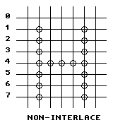
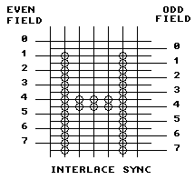
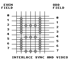
| x | 0 | Non-interlace |
| 0 | 1 | Interlace SYNC Raster Scan |
| 1 | 1 | Interlace SYNC and Video Raster Scan |
| Bit | Cursor mode | |
|---|---|---|
| 6 | 5 | |
| 0 | 0 | No Blinking |
| 0 | 1 | No cursor |
| 1 | 0 | Blink at 16x field period |
| 1 | 1 | Blink at 32x field period |
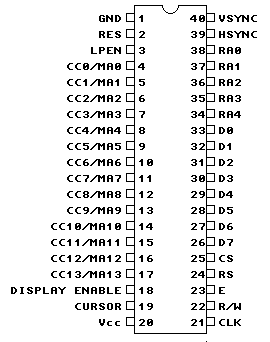
| /CS | RS | Address Register | Register No. | Register Name | Stored Info | RD | WR | Register Bit | |||||||||||
|---|---|---|---|---|---|---|---|---|---|---|---|---|---|---|---|---|---|---|---|
| 4 | 3 | 2 | 1 | 0 | 7 | 6 | 5 | 4 | 3 | 2 | 1 | 0 | |||||||
| 1 | - | - | - | - | - | - | |||||||||||||
| 0 | 0 | - | - | - | - | - | - | Address Register | Reg No. | Y | A4 | A3 | A2 | A1 | A0 | ||||
| 0 | 0 | - | - | - | - | - | - | Status Reg. | Y | L | V | ||||||||
| 0 | 1 | 0 | 0 | 0 | 0 | 0 | R0 | Horiz. Total | #Charac. -1 | Y | * | * | * | * | * | * | * | * | |
| 0 | 1 | 0 | 0 | 0 | 0 | 1 | R1 | Horiz. Displayed | #Charac. | Y | * | * | * | * | * | * | * | * | |
| 0 | 1 | 0 | 0 | 0 | 1 | 0 | R2 | Horiz. Sync Position | #Character. | Y | * | * | * | * | * | * | * | * | |
| 0 | 1 | 0 | 0 | 0 | 1 | 1 | R3 | VSYNC, HSYNC Widths | #Scan lines and #Char. Times | Y | H3 | H2 | H1 | H0 | |||||
| 0 | 1 | 0 | 0 | 1 | 0 | 0 | R4 | Vert. Total | #Char Rows.-1 | Y | * | * | * | * | * | * | * | ||
| 0 | 1 | 0 | 0 | 1 | 0 | 1 | R5 | Vert. Total Adjust | #Scan Lines | Y | * | * | * | * | * | ||||
| 0 | 1 | 0 | 0 | 1 | 1 | 0 | R6 | Vert. Displayed | #Char Rows | Y | * | * | * | * | * | * | * | ||
| 0 | 1 | 0 | 0 | 1 | 1 | 1 | R7 | Vert. Sync Position | #Char. Rows | Y | * | * | * | * | * | * | * | ||
| 0 | 1 | 0 | 1 | 0 | 0 | 0 | R8 | Mode Control | Y | I1 | I0 | ||||||||
| 0 | 1 | 0 | 1 | 0 | 0 | 1 | R9 | Scan Line | #Scan Lines-1 | Y | * | * | * | * | * | ||||
| 0 | 1 | 0 | 1 | 0 | 1 | 0 | R10 | Cursor Start | Scan line no | Y | B1 | B0 | * | * | * | * | * | ||
| 0 | 1 | 0 | 1 | 0 | 1 | 1 | R11 | Cursor End | Scan Line No | Y | * | * | * | * | * | ||||
| 0 | 1 | 0 | 1 | 1 | 0 | 0 | R12 | Display Start Addr (H) | Y | * | * | * | * | * | * | ||||
| 0 | 1 | 0 | 1 | 1 | 0 | 1 | R13 | Display Start Addr (L) | Y | * | * | * | * | * | * | * | * | ||
| 0 | 1 | 0 | 1 | 1 | 1 | 0 | R14 | Cursor Position (H) | Y | Y | * | * | * | * | * | * | |||
| 0 | 1 | 0 | 1 | 1 | 1 | 1 | R15 | Cursor Position (L) | Y | Y | * | * | * | * | * | * | * | * | |
| 0 | 1 | 1 | 0 | 0 | 0 | 0 | R16 | Light Pen Reg (H) | Y | * | * | * | * | * | * | ||||
| 0 | 1 | 1 | 0 | 0 | 0 | 1 | R17 | Light Pen Reg (L) | Y | * | * | * | * | * | * | * | * | ||
| * | Designates binary bit | Designates unused bit. These bits are always "0", except for /CS=1, which does not drive the data bus at all. |
| Register | UM6845R, MC6845, MC6845*1 | MC6845R, HD6845R | UM6845, HD6845S | UM6845E | SYS6545-1 | |
|---|---|---|---|---|---|---|
| R0 HTotal | Total-1 | Total-1 | Total-1 | Total-1 | Total-1 | |
| R1 HDisp | Actual | Actual | Actual | Actual | Actual | |
| R2 HSync | Actual | Actual | Actual | Actual | Actual | |
| R3 Sync Width | Horizontal (& Vertical *1) | Horizontal | Horizontal & Vertical | Horizontal & Vertical | Horizontal & Vertical | |
| R4 VTotal | Total-1 | Total-1 | Total-1 | Total-1 | Total-1 | |
| R5 VTotal Adjustment | Any Value | Any Value | Any Value | Any Value | Any Value Except R5 | |
| R6 VDisp | Any Value <R4 | Any Value <R4 | Any Value <R4 | Any Value <R4 | Any Value <R4 | |
| R7 VSync | Actual-1 | Actual-1 | Actual-1 | Actual-1 | Actual-1 | |
| R8 Mode Select | Bit 0, Bit 1 | Interlace | Interlace | Interlace | Interlace | Interlace |
| Bit 2 | - | - | - | Row/Column or Binary Addr. | Row/Column or Binary Addr. | |
| Bit 3 | - | - | - | Shared or Transparent Addr. | Shared or Transparent Addr. | |
| Bit 4 | (Display Enable Skew *1) | - | Display Enable Skew | Display Enable Skew | Display Enable Skew | |
| Bit 5 | (Display Enable Skew *1) | - | Display Enable Skew | Cursor Skew | Cursor Skew | |
| Bit 6 | (Cursor Skew *1) | - | Cursor Skew | RA4/ | RA4/ | |
| Bit 7 | (Cursor Skew *1) | - | Cursor Skew | Transparent | Transparent | |
| R9 Scan Lines | Total-1 | Total-1 | Total-1 | Total-1 | Total-1 | |
| R10 Cursor Start | Actual | Actual | Actual | Actual | Actual | |
| R11 Cursor End | Actual | Actual | Actual | Actual | Actual | |
| R12/R13 Display Addr. | Write-Only, Read/Write (MC6845 & *1) | Read/Write | Read/Write | Write Only | Write Only | |
| R14/R15 Cursor Position | Read/Write | Read/Write | Read/Write | Read/Write | Read/Write | |
| R16/R17 Position | Read-only | Read-only | Read-only | Read-only | Read-only | |
| R18/R19 Update Addr. Register | N/A | N/A | N/A | Transparent Mode Only | Transparent Mode Only | |
| R31 Dummy Register | N/A | N/A | N/A | Transparent Mode Only | Transparent Mode Only | |
| Status Register | Yes (UM6845R) | No | No | Yes | Yes | |
| Register | UM6845R, MC6845, MC6845*1 | MC6845R, HD6845R | UM6845, HD6845S | UM6845E | SYS6545-1 |
|---|---|---|---|---|---|
| R0 HTotal | Total-1 = Odd or Even | Total-1 = Odd | Total-1 = Odd | Total-1 = Odd or Even | Total-1 = Odd |
| Register | UM6845R, MC6845, MC6845*1 | MC6845R, HD6845R | UM6845, HD6845S | UM6845E | SYS6545-1 |
|---|---|---|---|---|---|
| R4 VTotal | Total-1 | Total-1 | Total-1 | Total-1 | Total/2-1 |
| R6 VDisp | Total | Total/2 | Total | Total | Total/2 |
| R7 VSync | Actual-1 | Actual-1 | Actual-1 | Actual-1 | Actual/2 |
| R9 Scan Lines | Total-1 Odd/Even | Total-1 Only Even | Total-1 Odd/Even | Total-1 Odd/Even | Total-1 Odd/Even |
| R10 Cursor Start | Odd/Even | Both Odd or Both Even | Odd/Even | Odd/Even | Odd/Even |
| R11 Cursor End | Odd/Even | Both Odd or Both Even | Odd/Even | Odd/Even | Odd/Even |
| CCLK | 2.5Mhz | 2.5Mhz | 3.7Mhz | 3.7Mhz | 2.5Mhz |
| Part Number | CPU Clock Rate | Package |
|---|---|---|
| UM6845R | 1Mhz | Plastic |
| UM6845RA | 2Mhz | Plastic |
| UM6845RB | 3Mhz | Plastic |