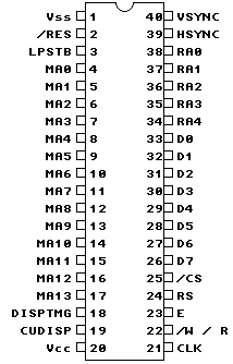
| Register #
| Register Name |
Anomalous opeations caused by rewriting registers & Conditions to avoid those operations |
Rewriting** OK or NG |
| R0 |
Horizontal Total |
The horizontal scan period is disturbed. |
X |
| R1 |
Horizontal Displayed |
There are some cases where the width of DISPTMG becomes shorter than the programmed
value at the moment of the rewrite operation. An error operation occurs only during one
raster period. |
O |
| R2 |
Horizontal Sync Position |
There are some cases where HSYNC is placed on the position different from the programmed
value or the noise is output. |
X |
| R3 |
Sync Width |
When a rewrite operation is performed at a "High" level on HSYNC
pulse or VSYNC pulse, there are some cases where the width pulse becomes shorter than
the programmed value at the moment of a rewrite operation.
|
/\ |
| R4 |
Vertical Total |
When a rewrite operation is performed during the last raster period in the line, there
is a possibility that the disturbance occurs during the vertical scan period.
There is no problem of a rewrite operation during raster period except this period.
|
/\ |
| R5 |
Vertical Total Adjust |
When a rewrite operation is performed in the last character time of the raster period,
there are some cases where the numbers of Adjust Register, specified by program, are
not added. (Only during the adjust raster period). |
/\ |
| R6 |
Vertical Displayed |
After the moment of a rewrite operation, there are some cases where
the Display is inhibited. However, the display according to the programmed
value is performed from the next field. |
O |
| R7 |
Vertical Sync Position |
There are some cases where VSYNC is placed on the position different from
the programmed value or the noise is output. |
X |
| R8 |
Interlace & Skew |
Neither scan mode bit nor skew bit is rewritten dynamically. Dynamic Rewrite into scan mode bit and skew bit is prohibited. |
X |
| R9 |
Maximum Raster Address |
The internal operation will be disordered by a rewrite operation. |
X |
| R10 |
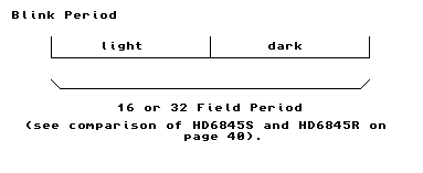
Cursor Start Raster |
When a rewrite operation is performed in the last character time of the raster period,
there are some cases where the jitter occurs on the cursor raster or the cursor
is not displayed correctly. There is also a possibility that the blink rate becomes
temporarily shorter than usual. |
/\ |
| R11 |
Cursor End Raster |
When a rewrite operation is performed in the last character time of the raster period,
there are some cases where the jitter occurs on the cursor rraster or the cursor
is not displayed correctly. Moreover, there are also some cases where the blink rate
becomes temporarily shorter than normal operation. |
/\ |
| R12 |
Start Address (H) |
R12 and R13 are used in the last raster period of the field. A rewrite operation can
be performed except during this period. However, when R12 and R13 are rewritten
in each field seperatly, the display operation, whose start address is determined temporarily by
programming sequence, will be performed. A rewrite operation should be performed during the horizontal/vertical
display period. |
O |
| R13 |
Start Address (L) |
O |
| R14 |
Cursor (H) |
When a rewrite operation is performed during the display period,
there are some cases where the cursor is temporarily displayed at the address different from
the programmed value. A rewrite operation should be performed during the horizontal/vertical
retrace period. Also, when R14 and R15 are rewritten in each field seperatly, the cursor
is displayed temporarily at the temporal address by programming sequence. |
O |
| R15 |
Cursor (L) |
O |
| No. |
Functional Difference |
HD6845R |
HD6845S |
| 1 |
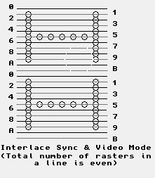
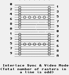
Interlace Sync & Video Mode Display |
Programming Method of Number of Vertical Characters |
In HD6845R, number of characters is vertically programmed in a unit
of two lines, as illustrated above. (Number of vertical total characters,
Number of vertical displayed characters, Vertical Sync Position).
Example of above figure
Programmed number into Vertical Display
Register = 5 |
In HD6845S, number of characters is vertically programmed in a unit
of one lines, as illustrated above. (Number of vertical total characters,
Number of vertical displayed characters, Vertical Sync Position).
Example of above figure
Programmed number into Vertical Display
Register = 10 |
| Number of Rasters per Character Line |
Only even number can be specified. |
Both even and odd number can be specified |
|
|
|
|
Number of raster = 10 scan-line (specified) |
When number of raster per character line is EVEN. Number of raster = 10 scan line (specified) |
When number of raster per character line is ODD. Number of raster = 9 scan line (specified) |
However, number which is programmed into register is calculated as follows.
Programmed number (Nr) = (Number specified)-1 |
However, number which is programmed into register is calculated
as follows:
Programmed number (Nr) = (Number specified-2) |
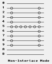
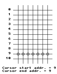
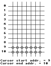
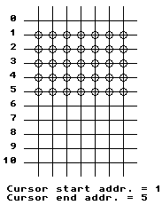
| Cursor Display |
Cursor is displayed in either EVEN field or ODD field
![[Example 1]](hd10.gif)
![[Example 2]](hd11.gif)
|
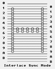
Cursor is displayed in both EVEN and ODD field
![[Example 1]](hd12.gif)
![[Example 2]](hd13.gif)
![[Example 3]](hd14.gif)
|
| 2 |
Vertical Sync Pulse Width (VSYNC output) |
Fixed at 16 raster scan cycle (16H) |
Programmable (1-16 raster scan cycle |
| 3 |
SKEW function |
Not included |
SKEW function is newly included in DISPTMG, CUDISP signals |
| 4 |
Start Address Register |
Impossible to READ |
Possible to READ |
| 5 |
RESET signal (/RES) |
MA0-MA13 Output, RA0-RA4 - Synchronous Reset
Other Outputs - Asynchronous Reset
Output signals of MA0-MA13, RA0-RA4 synchronising with DLK "low"
level, go to "low" level after /RES has gone to "low".
Other outputs go to "low" immediatly after /RES has gone
to "low"level.
|
MA0-MA13 Output, RA0-RA4, Other Outputs - Asynchronous Reset
Output signals of MA0-MA13, RA0-RA4 and others go to "low"
level immediatly after /RES has gone to "low" level.
|